
How to use VIZO:
A visual language for interacting with the board
VIZO is not a chatbot for generic conversations, but a graphical engineering tool. You interact with the system using colored arrows, measurement markers, and selection frames directly over the PCB photo or schematic diagram.
Diagnosis in 3 simple steps
1. Put a board or schematic on the bench
Click «+» at the bottom of the screen: take a camera shot, pick a photo from gallery, or attach a PDF schematic / Boardview file.
2. Place an arrow or a measurement
Point an arrow at a suspect chip or record voltage with a pin marker (for example, 19V, 0V).
3. Launch node analysis (->)
The system will extract the pinout from documentation, compute PWM startup conditions, and provide verified solutions.
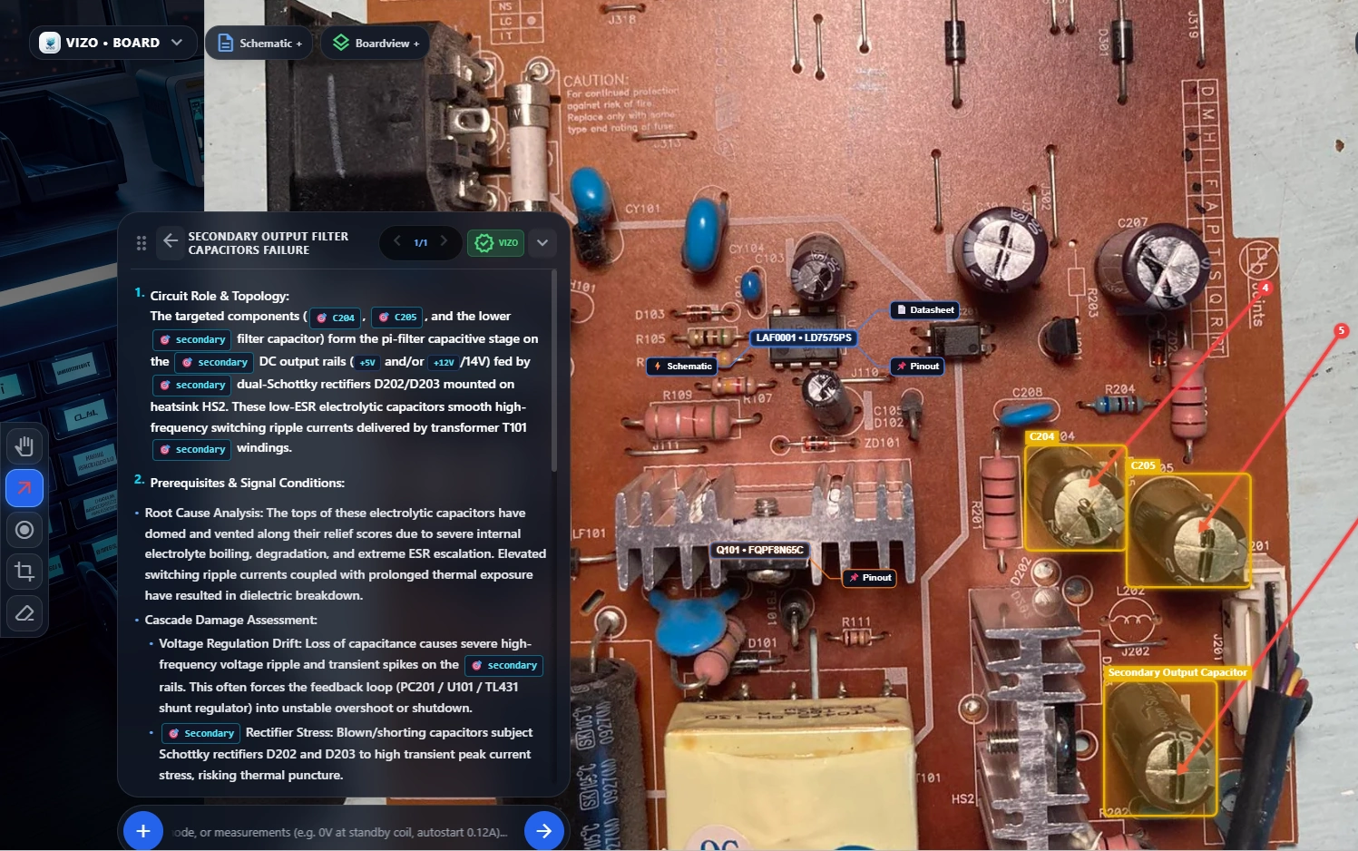
What arrow and pin colors mean
Every action by the technician on the canvas passes typed spatial vectors into the VIZO core. Below is the system response and UI result for each tool.
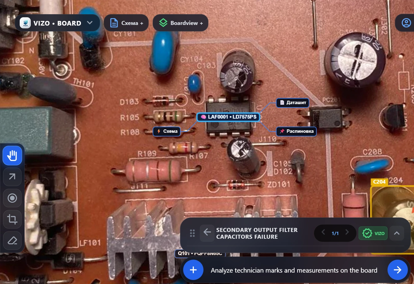
Used to identify components. Point the tip at a part — VIZO recognizes the laser marking, explains its circuit role, and attaches the factory pinout crop.
SnapEngine resolves RefDes in Boardview. SkiaMacroCropper generates a high-res crop. The Librarian agent validates the MPN, queries distributor catalogs, downloads factory PDF, and extracts the pinout.
Interactive chip callout appears with [Pinout], [PDF], and [Analogs] badges. The card provides pin-by-pin functions and operating voltages.
Indicates a node under inspection. The system generates an in-circuit multimeter procedure without desoldering: diode-mode voltage drop (mV), resistance to GND, and control thresholds.
AI Architect calculates node physics, power rails, pull-up/pull-down dividers, and forms a non-destructive test sequence without removing components.
Yellow bounding box on the PCB. The card details diode-mode drops (mV), resistance to GND (Ω), and expected enable signals.
The component is verified failed. The system isolates the shorted rail, highlights the connected power bus, and identifies components at risk of cascade breakdown (high/low-side FETs, downstream loads).
System skips re-inspection. It traces backward for root causes (VIN surges, gate driver runaway) and forward for downstream cascade damage.
Red box around defective component. Diagnostic card presents pre-soldering risk checklist (gate driver, high-side FET, load shorts).
Mark a verified, properly operating circuit node.
Node is committed to ProvenHealthyNodes facts. The model excludes it from further failure hypotheses and advances along the Power Sequence.
Green healthy badge. The diagnostic card proceeds to the next stage in the startup sequence.
Placed on a test point or chip lead with a specified voltage (e.g. 19V, 0V). When 0V is recorded on a rail, the system provides a structured diagnostic checklist: controller start conditions (EN/VCC), load resistance to GND, and current sense circuits.
Live OSNAP magnetically snaps reading to CAD pad. Reading is treated as Ground Truth. If 0V or anomalous voltage is detected, system calculates causes (open pull-up, protection trip, shorted load).
Orange badge with exact voltage right on the pin. Card provides circuit analysis explaining voltage drops and root causes.
Select dense SMD clusters or intricate schematic areas using a rectangle.
Client extracts full-resolution crop without downscaling entire board. SpatialFrameAggregator identifies all components inside bounding box and feeds them as a unified cluster.
AI analyzes multi-component interactions concurrently (e.g. full charger support circuitry) without losing optical line sharpness.
How to achieve 0.2 mm CAD alignment precision on any smartphone camera
VIZO utilizes an 8-DOF Direct Linear Transformation (DLT Homography). Moving one control point recalculates perspective across the entire board. To align CAD pads with QFN 0.4–0.5 mm lead pitches, use the iterative 3-pass method:
At full view, align the 4 reticles with outer PCB corners or mounting screw holes (H1..H4).
Zoom in and align reticles with pin 1 of corner ICs clockwise: TL → TR → BR → BL.
Final verification loop. Use Right Mouse Button (RMB) to instantly pull the nearest corner under your cursor without scrolling.
Signal and power rail tracing (Signal Tracer)
VIZO features a built-in topological visualization engine that transforms static netlists into directed energy flows with animated current particles passing through series components and jumping across board layers.
Traces originate from physical sources (connector JDCIN, IC output) through 2-pin passives (PL402.1 → PL402.2) to loads. Glowing neon particles indicate current direction at 60 FPS.
When a signal dives into internal layers, the line does not break. The engine locates the nearest via (VIA), renders a pulsing purple ring, and casts an X-ray dashed ray to the reverse side component.
Main power rails (19V / 3.3V) display in cyan, while PWM controller gate-drive signals display in separate green rays. You immediately see where gate switching pulses originate.
Signal trace color coding:
Anatomy of an interactive part callout
VIZO intentionally disables background bulk-loading of datasheets for all board components to maximize responsiveness and keep the AI context clean. Basic mode operates instantly on internal engineering memory. When a node is in a «gray zone» (voltage is abnormal), click the chip name and toggle 🧠. The factory PDF becomes an absolute anchor of truth, matching your readings against the manufacturer's Electrical Characteristics down to the millivolt.
Click the chip name to enable the brain icon. The next question automatically sends the full pin table of that IC into the model context.
Opens the official manufacturer PDF in the built-in viewer, including offline support on phones.
Click to expand a datasheet crop of the package with pin numbers (QFN, SOIC, TO-220) and names (VIN, GND, BOOT, EN).
A list of 100% compatible chips from other brands when the original IC is not in the shop.
VIZO engineering tips
Worn-off chip marking
If the package is burned or covered in coating, pick the Pin tool, tap the chip body, and type the likely part number (e.g. TPS51125). The model will fetch docs from your text.
Dense schematics and crossings
If the drawing is a thick mesh of crossing lines, select the suspect node with Crop. The model gets a high-resolution crop so the lines do not smear.
Follow-up questions in the bar
Do not clear the board for a new question. Type below: “Pin 3 is only 0.4V instead of 1.8V, why?” — VIZO will compute the divider in front of that pin.
Controlling the workbench on PC and phones
- Mouse wheel Smooth zoom around the cursor
- Hold LMB (Hand) Pan the board on the table
- Double-click Reset zoom to 1:1
- Escape Clear the crop box
- Enter Send the measurement for analysis
- Two-finger pinch Pinch-to-zoom
- One-finger swipe Pan the board in Hand mode
- Double-tap Reset zoom
- Swipe a card left/right Flip hypotheses and fixes
- Swipe the PDF window down Quickly close the datasheet
Ready to test it on your board?
Open the workbench, load the first board, and see how fast datasheet crops and node analysis feel.
Go to the workbench arrow_forward